 The 2D0 is Tech Edge's original OEM wideband product.
As of 2008 the LSU 4.0/4.2 & the LSU 4.9 may be used with the 2D0 (but note: firmware differs).
The 2D0 is Tech Edge's original OEM wideband product.
As of 2008 the LSU 4.0/4.2 & the LSU 4.9 may be used with the 2D0 (but note: firmware differs).
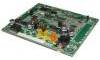
There is a newer surface mount version 2D1 with smaller footprint and extra features.
We designed 2D0 primarily for integration into other manufacturers
equipment but it's also suitable for other applications
where other unit's in-built logging features are not required.
2D0 does not include conditioned RPM, thermocouple, and user logging channels
and it uses the lower cost DIP-28 ATMega-8 processor.
2D0 includes the enhanced pump cell control technology found in all newer version 2.0 units.
Note : 2D0 does have a raw, or unconditioned, user (P1)
and pulse input (P3) on two PCB points (see details below).
 We can, and have, customised the basic 2D0 design for specific OEM applications, interfaces and environments.
Contact us for more information.
We can, and have, customised the basic 2D0 design for specific OEM applications, interfaces and environments.
Contact us for more information.
![]() from March 2011
we have a boxed and finished version of the newer 2D1 controller board.
The 2DP Professional model is presented in a diecast metal case and comes standard with 4-20mA loop capability.
from March 2011
we have a boxed and finished version of the newer 2D1 controller board.
The 2DP Professional model is presented in a diecast metal case and comes standard with 4-20mA loop capability.
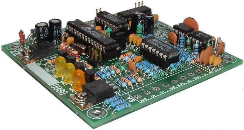
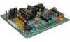
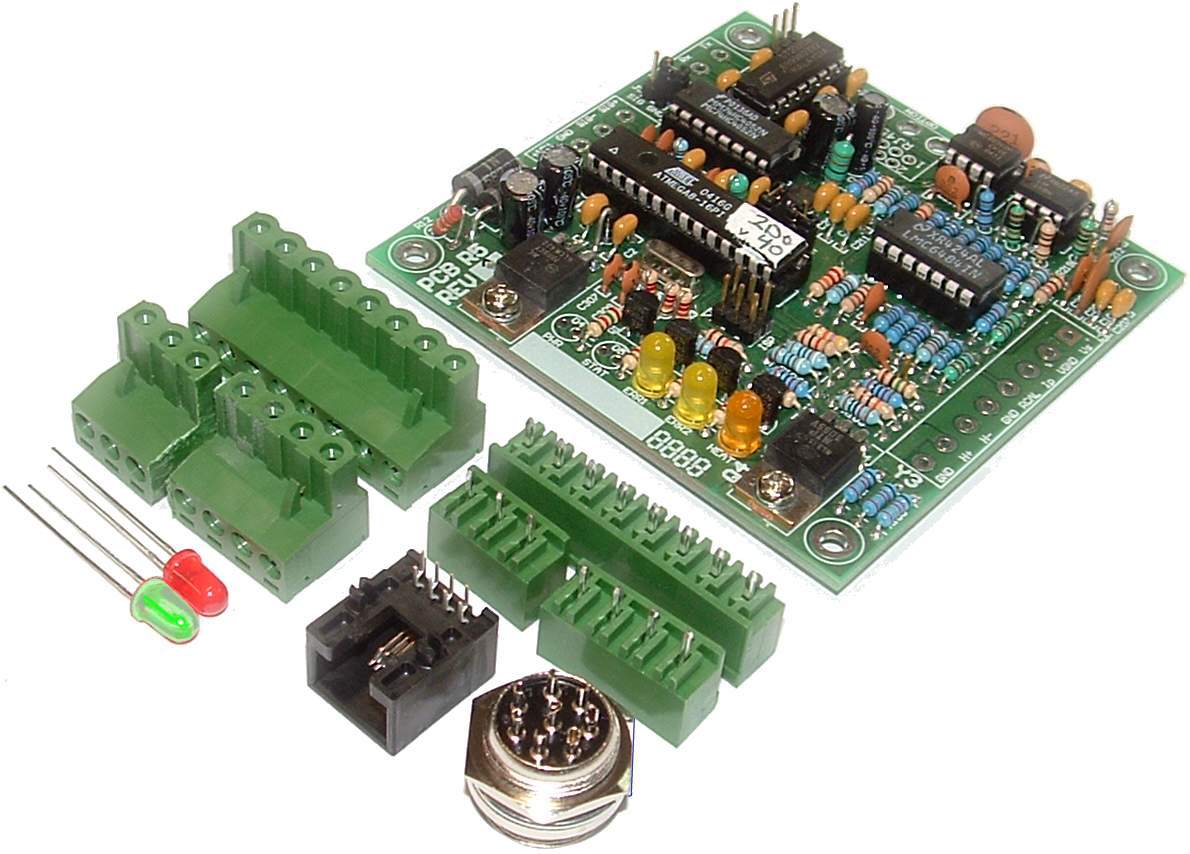
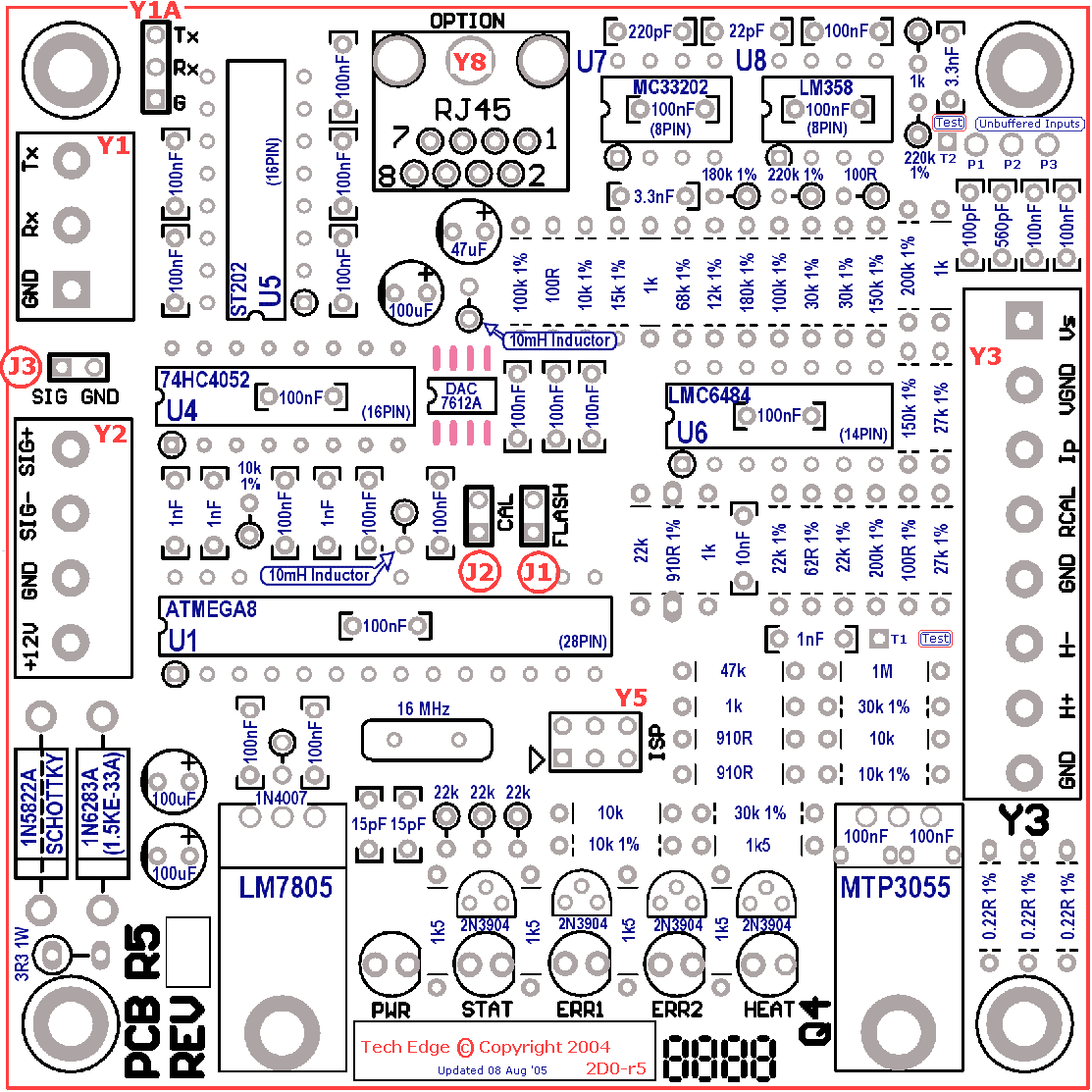
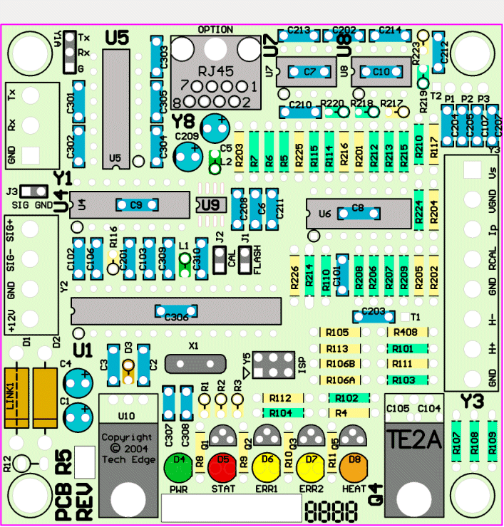
As you can see it's fairly small (click on the image to enlarge it or go here to see it in plan view). 2D0 uses through hole components for ease of in-field service although there will be a future smaller surface mount version. PCB dimensions are 85 x 85 mm and less than 20 mm high (~33/8" per side, and <3/4" high). See also the component value overlay and the component ID overlay.
Other features include:
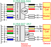
The 2D0 Wideband unit, in its basic form, comes as a pre-built and tested PCB without connectors. It has the facility for 3 connectors of 5.08 mm (0.2") pitch and a single RJ45 connector. The connector functions listed in blue, the markings found on the PCB are shown in (italic red):
See the LSU information pages or the full schematics for the 6066 & 7057 cables. The 7 output lines must go to a circular 8 pin connector if it is to be used with a standard WBo2 cable. |
 |
||
Vs | [1] Vs | Sense cell Voltage to WBo2 |
|
Vs/Ip | (2) VGND | Common for Vs/Ip | |
Ip | (3) Ip | Pump cell current from WBo2 | |
Rcal | (4) RCAL | Calibration resistor from sensor | |
Ground | (5) GND | Cable shield | |
H- | (6) H- | Heater negative | |
H+ | (7) H+ | Heater positive | |
Ground | (8) GND | Extra GND | |
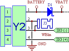
Power supply must be able to supply up to 3 Amps at 12 Volts. Operating current is typically 1 Amp with sensor at room temperature. The J3 shunt (marked SIG GND) is described below. |
 |
||
VBatt | [1] +12V | Battery - 10.5 to 19.5 Volts, reverse protected | |
Ground | (2) GND | Ground or Battery negative | |
WBlin- | (3) SIG- | Wideband floating GND output | |
WBlin+ | (4) SIG+ | Wideband Output, 0 to 5 Volts | |
A standard 0.2" (5.08 mm) connector is used. There is a permanently installed 0.1" header Y1A (for factory testing) which is a duplicate of the 3 pin connector Y1, and is located behind it. |
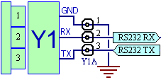 | ||
Ground | [1] GND | Rx/Tx return |
|
Rx | (2) Rx | Receive line from PC | |
Tx | (3) Tx | Transmit line to PC | |
This is the RJ45 connector with standard WBo2 pinouts for the pins used. It mates with the PC RS232 cable or the LD01/LD02 display. |
) | ||
SVout | [1] SVout | LD01 analogue (10 bit PWM) output. |
|
Rx | (2) Rx | Receive line from PC | |
Tx | (3) Tx | Transmit line to PC | |
Ground | (5) GND | Ground return | |
VBatt | (8) +12V | Current limited (3R3 resistor) battery power | |
No connector is used but there are three labelled pins on the PCB in the top right hand corner. Note that a 0.1" header can be soldered there. |
) | ||
| P1 | USER | ADC Input, unbuffered | |
| Ground | GND | Return data path | |
| P2 | PULSE | Timer measures duration | |
2D0 Purchase Options
2D0 was designed to be a low cost unit that is integrated into other devices.
This often means using special connectors with point to point wiring.
The 2D0 module can be supplied with or without connectors.
(refer to the The circular male 8 pin connector is the same as that found on other version 2.0 WBo2 units and is, solder bucket style & panel mount with the nut and washer behind the panel. This connector mates to a female 8 pin that is on the WBo2 end of the sensor cable. These cables are available in a few standard lengths (2.6 m & 4.0 m are the most popular). An additional RS232 cable (with RJ45 and DB9 connector) for PC communications is available separately. |
)
Jumper Shunts J1, J2, J3Jumper shunts J1 & J2 are located at the centre of the board, J3 is located between pins 3 and 4 of the 0.2" headers. Click to enlarge the image. J1 - (FLASH) should normally be OFF except when using the rescue re-flash function to update on-board firmware, and only then if there is a corruption of main program memory. Refer to WButil.exe for details and HXF files. J2 - (CAL) should normally be ON at all times, and is used for factory calibration and testing Note that free-air sensor calibration is quite different and is done using the WButil.exe utility. J3 - (SIG GND) provides a link between the SIG- output and GND and is used when a single ended output (this is WBlin+ on the SIG+ pin) is required. Remove J3 when differential output is required, but in this case ensure WBlin- on the SIG- pin is connected to the destination input's GND_d point. For differential output there should not be more than a Volt of so difference GND_d and the 2D0's GND point. This topic is discussed further here. |
WBlin+ Pin 4/Y2 & WBlin- Pin 3/Y2 Wideband Output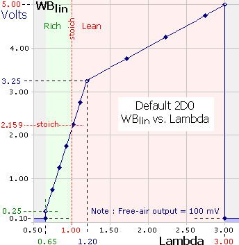
The WBlin output on 2D0 has default values a little different to other WBo2 units.
Remember that the WBo2 configuration program WButil.exe lets you change these defaults.
Rather than the default linear AFR = 9.0 to 19.0 span of WBo2's standard 0 to 5 Volt output (see it here), 2D0 has a Lambda=0.65 to 3.0 span (*) over the 0.25 to 5.0 Volt range in two linear segments centered about Lambda = 1.2 at 3.25 Volts. This is shown in the graph at right. (* equivalent AFR range is 9.56 to 44.1). The effect of this is to reduce the resolution of the rich tuning range (AFR=9.6 to 17.6 covers 3.0 Volts) at the expense of better resolution in the lean range. The actual formula for the dual slope follows the general straight line formula y=mx+c. In the formula below, L is Lambda, and V is voltage:
Note very carefully, the rich graph starts at Lambda = 0.65 and a voltage of 0.25 Volts. The lean graph ends at a Lambda of 3.0 and Voltage of 5.0. Outside that range you should consult the next paragraph on Bounded Output. Lastly, note that stoich (ie. Lambda = 1.0) has a voltage of 2.159 Volts. To convert the above formula to AFR, remember that:
Bounded OutputAnother 2D0 feature is the setting of valid Lambda limits by clamping WBlin to a fixed voltage when Lambda is higher or lower than the bounding limits. This scheme allows a recording device to determine if the WB output is valid (must be greater than 100 mV). The default Lambda bound limits are 0.65 and 3.0 and a bounding Voltage of 100 mV. If Lambda is richer or leaner than these values then WBlin will be fixed at 100 mV. In the image at right this is shown as the grey area to either side of the light green (rich) and the pink (lean) range. The actual clamped value is shown down the bottom in the light blue region. It's possible to change the clamp values for 2D0 by modifying configuration parameters. The WButil.exe program is run, and in the Comms tab the following commands are manually entered in the Command box. The same program can re-program the output table(s) from the AFR Tables tab. This sequence defeats the clamping action by setting the rich Ipx threshold limit to 0 and the lean limit to 0x3000.
Remember that if you re-flash the WBo2 unit with newer firmware, the setting entered above will be lost. |
SVout Pin 1/Y8 (on RJ45) Compatibility Output
The SVout signal is intended for analogue displays like the LD01 but can be used as an alternate, lower resolution, single ended output. To generate SVout, the processor uses a 65 word lookup table with linear interpolation. It converts the normalised pump current (Ipx) into a 10 bit value representing SVout. A hardware PWM (Pulse Width Modulation) pin on the processor generates the actual SVout voltage. SVout is compatible with the Vout signal from the original oz-diy-wb unit (and the 1.5 unit's Vwb). It can be used to drive the analogue LD01 display (or the older 5301 if you change its connector). The default SVout, shown at right, varies between about 1.0 Volt for a very rich mixture (Lambda=0.6 or AFR=9), to 2.50 Volts for a stoic mixture, and to 3.1 Volts for a lean mixture (AFR=25). In free-air the SVout should be exactly 4.00 Volts when the unit has been free-air calibrated correctly. The default AFR vs. SVout relationship is shown in the Vout table/graph page. The analogue Vout is a continuously available signal that may be logged with a high speed logger. We recommend at least a 10 bit converter for best accuracy, but as the measuring range is small (less than 3 Volts), measuring resolution is reduced compared to using a smaller AFR range over a larger voltage range. |
|
|
Note that as well as the three RS232 signals on Y1, for convenience, the RJ45 connector (Y8) also carries those same signals. click on the image to see the way the RJ45 is numbered. The 2D0 unit transmits logged data (Lambda/AFR and the analogue and pulse inputs) on its Tx line [pin 3] and receives commands (from PC or display) and code updates from a PC on its Rx line [pin 2]. The diagram at left shows the wires within the cable and also the connections at each end. Note the pin names change from left to right - the 2D0 unit's Tx pin transmits to the PC's Rx pin (and vice versa). [pin 1] is the shield for the Rx and Tx data lines as well as being the return data path. |
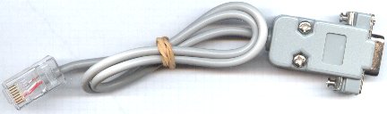
WBo2 to PC cableHere's an image of the actual RS232 cable for connection between a PC and 2D0's RJ45 connector. The cable is used for either logging to a PC, or for re-flashing its code (under control of a PC). If you need to extend the cable then a standard straight through male-female DB9 extension cable should be used (ie. not a cross-over or null modem cable). |
|
)
Serial Data logging - Lambda, Analogue & PulseAs noted above, as well as the Lambda/AFR input the unit produces, there are two extra inputs ..
.. that can be logged, although no buffering is provided for these inputs. The actual output is logged in a data frame that is fully described in the logging information section (default frame type is 1). The pins of the PCB for the inputs are shown in the diagram at right or can be found in the top right hand corner of this popup overlay and labelled unbuffered inputs. |
Due to user demand we have added an Auto-Calibrate feature that enables a button press sequence to automatically perform a free-air calibration. This allows the wideband unit to be periodically calibrated without external software nor PC connectivity. Adding this feature to existing units is as simple as adding a couple of components and a button, and also updating the unit's firmware. The advantage is that more frequent calibrations can be performed more easily. Note that frequent re-calibrations carry with it the risk of de-calibrating the unit if steps are not taken to ensure the sensor is sitting in perfectly clean air each time a calibration is performed. If air at other than 20.9% oxygen content (ie. free-air) is used, or if large amounts of gaseous hydrocarbon are also preset, then the unit will not be correctly calibrated after the Auto-Cal operation.

The Auto-Calibrate feature eliminates the need for a PC to be used to calibrate the controller to a new sensor. A simple button press is used to start this free-air calibration process. Firstly ensure the sensor is sitting in perfectly clean air each time a calibration is performed. There is more information here on LSU sensor positioning that should also be consulted. If air at other than 20.9% oxygen content (ie. free-air) is used, or if large amounts of gaseous hydrocarbon are also preset, then the unit will NOT be correctly calibrated after the Auto-Cal operation.
Software : Firmware version 0652 or higher is required. Go to the HXF files page to download the latest files. The v command can be used to determine the firmware revision. The re-flash utility will automatically show the firmware version.
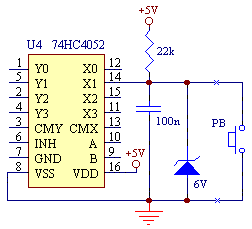
Hardware : A button, and de-bounce circuitry to initiate Auto-Cal, must be added.
Refer to the schematic at right with a 22k pull-up resistor (any value from 10 k to 100k should work fine)
and de-bounce capacitor (10 nF to 100 nF or 0.01 uF to 0.1 uF).
The actual button goes across the de-bounce capacitor.
Also shown is an optional zener diode (only needed for very long cable runs to the button)
and is designed to prevent spikes getting into the button circuitry.
See also the ![]() Fixes
section for more details of the hardware required.
Fixes
section for more details of the hardware required.
Note that the newer 2D1 model already includes the de-bounce and anti-static parts.
Operation with firmware 0658 or higher: Press the Auto-Cal button for at least 1.5 seconds and no more than 4 (this is to avoid false triggering and also continuous operation with a stuck button - count 0, 1, 2 while holding the button). The red LED will begin fast flashing at about 4 flashes/second. If the sensor is in stable free-air then after After 15-20 seconds the LED will do three slower flashes indicating completion of the operation. At this point the free-air calibration value has been calculated and saved. You must perform the Auto-cal operation again if it did not succeed, or it was performed inadvertently. The animated image at above right shows this - it takes almost 20 seconds to complete!
Advanced users should note that the Ipx-scaling value, being the result of the Auto-cal operation, resides at config memory address 0x3B (low byte) and 0x3C (high byte). The g3b and the g3c commands display these two bytes.
|
We suggest you update to firmware 0658 or higher, so this section if for reference purposes and applies only to the 0652 firmware. Operation with firmware 0652: Press the Auto-Cal button for at least 4 seconds, or until the red LED begins a fast flashing to indicate it's performing an Auto-Cal. If the sensor is in stable free-air then after 15 seconds the LED will do a slower flash indicating completion of the operation. At this point the free-air calibration has been calculated but not saved. There are two options
After either operation, the red LED will return to showing status (normally this will mean being on solid). Note that if you don't see the amber heater LED doing a short quick flash, then the new calibration value has not been saved. If the new value is not saved, to retrieve the old calibration value, simply cycle the power to the 2D0 unit, and it will reload the previously saved value. |
LSU 4.9 support (added April 2008)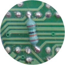
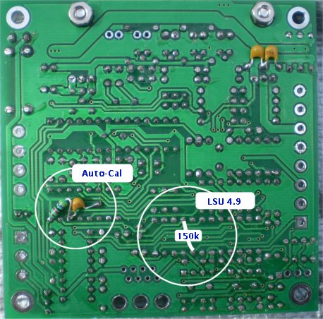
The image shows the 150k ohm resistor that should be added to the underside of the 2D0 board to add support for the LSU 4.9 sensor. This resistor supplies the necessary bias current. and runs between Vs and +5 Volts - it must be removed if you revert to an LSU 4.0/4.2. Remember that you also need different firmware for the LSU 4.9 sensor that operates the heater at a different impedance and has other specific modifications. The firmware is available from the HXF files section. WARNING : Operating the LSU 4.9 with LSU 4.2 firmware will result in the heater being over driven and short sensor life or even sensor destruction. Using the LSU 4.2 with 4.9 firmware will also result in inaccurate results but, importantly, too-low heater temperature which may also shorten its life as it cannot burn off impurities. The image also shows another shot of the parts for the 2D0 Auto-Cal modification. |
The 2D0 unit is software compatible with the other version 2.0 units and calibration and configuration software is available, but take particular note of the configuration software.
)
)
)
)
)
)
)
)
)
)