
 The LD02B DIY display (described here) was introduced in Dec. 2009 and replaces the LD02 kit.
The LD02B is also sold as a pre-built unit.
The LD02B DIY display (described here) was introduced in Dec. 2009 and replaces the LD02 kit.
The LD02B is also sold as a pre-built unit.
Changes from LD02 - We could not source the original through-hole Toshiba driver chip we had been using for the original DIY LD02 unit
so we redesigned the board and added some features.
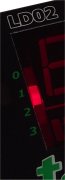
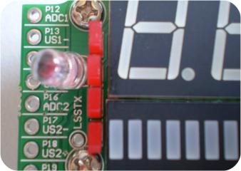
LD02B adds 4 rectangular LEDs that indicate which of the 4 views is active (see a representation of this at right).
A phototransistor is also used instead of an LDR for ambient light level sensing (for automatic dimming).
Changes to the local voltage and RPM/Vss inputs are also implimented.

Because LD02B uses some surface mount components, it comes as a partially built kit and requires minimal soldering.
The parts that must still be soldered include the LEDs and photo-transistor, buttons and some sockets, cabling, etc.
The DIY kit includes all parts (case, perspex cover, cable, PCB, all parts, etc.) including the re-programming adaptor.
You have to add solder, some glue, and time to construct it.
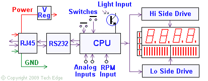
The image at left shows how the major components of the complete LD02 unit fit together.
Starting from the left is the RJ45 connector carrying power (& GND) to the unit as well as RS232.
The RS232 interface uses an ST HIN202 (like the ST202 or MAX232 chips).
This is a bi-directional interface and the Tx line allow the unit to handshake with a PC for re-programming.
The Atmel Mega-8 CPU interprets the data frames from WBo2 and reads the
two
|
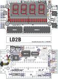
Component OverlayAt left is a thumbnail of the parts overlay showing the location of all parts on both sides of the PCB. Here is the Overlay as a PDF |
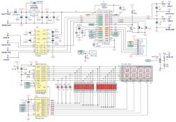
SchematicAt right is a thumbnail of the LD02B basic version schematic This version provides all the functionality of the original LD02 but adds the 4 view-indicator LEDs. Here is the schematic as a PDF |
Main PCB and associated parts 1 Pre-built PCB - id: LD02B (79x46mm) 1 * 4-digit 7-segment LED module 2 * 10-segment bar-graph LED modules 4 * rectangular LEDs (~4mm x 1.5mm) 1 5mm clear lens phototransistor 1 HIN202CP RS232 driver chip 1 ATMEG8-16PU Atmel CPU 2 long shaft (13mm) press buttons 1 16-pin DIP socket 1 28-pin DIP socket 1 2-pin 2mm header (rescue-reflash) 1 2mm shunt (rescue-reflash) 4 M3x6mm round (cheese) head chromed bolts 4 M3x15mm hex nylon spacers 1 prebuilt cable with clear RJ45 plug 1 Heatshrink (≈17mm long) Φ3mm, & Φ6mm |
Case and Other Hardware 1 milled plastic case 80x52mm 1 drilled plastic back/lid 1 * milled acrylic lens 1 LD02 te WIDEBAND adhesive faceplate 4 M2x18mm Philips-head black screws 4 rubber blanking plugs (black screw covers) 4 M3x6mm round (cheese) head chromed bolts 1 100mm (small) cable tie Reprogramming Adaptor 1 small PCB id: TE-SER01 (15x14mm) 1 Black 8-pin RJ45 PCB mount 90 degree socket 1 White 2-pin molex 90 degree Mini-Fit socket 1 DB9S female RS232 connector, solder bucket pins |
|
Colour Note* : The kit comes in two colours, red and green. The LED modules may also contain one of two possible LED families (BQ or FYQ) depending on manufacturer. |
|
|
4 x 7 segment common cathode display
Red: BQ-N516RD, or FYQ-R1025ZS-11
|
10 x bargraph linear display
Red: BA-10S1UD, or FYA-R102510ZS-11
|
)
Here is an image of all parts supplied in the LD02B DIY kit. The image shows three main groupings:
The parts are supplied in a number of sealed sections. All the small parts are grouped into one single bag. The semiconductors (except the phototransistor and rectangular LEDs) are inserted into an aluminium covered polystyrene block. The main board and screen are packed into the case.
UNPACKING :
|
)
|
LED ORIENTATION
|
)
|
|
ConstructionCorrect orientation and component height is the key critical construction issue for best results. Following this guide will help getting it right. Hopefully the diagrams are self explanatory. After checking the pre-tested PCB for any faults that may have developed in transit ...
|
|
|
|
|
|
|
|
|
|
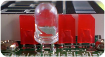
This is another shot of the phototransistor and rectangular LEDs showing how the phototransistor naturally points out at about a 60° angle. )
|
)
|
This shows the top button installed. Click on the image for an alternate enlarged image of both buttons.
Locate the back of the case - it has four pre-drilled and countersunk holes.
The four countersunk M3 bolts can be used to secure the display assembly to the case back.
|
|
|
|
|
|
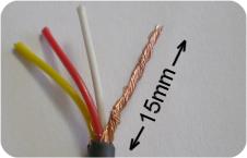
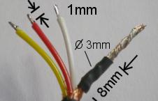
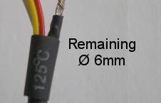
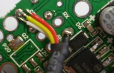
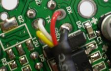
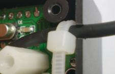
The prepared cable is now soldered to the PCB. Remove the nylon spacer for better access to the area. Insert the braided conductor into the GND hole. Insert right up to the heat shrink, and solder on the other (component) side - then cut off the exposed copper braid. this will leave the coloured wires much longer than the insulated braided copper. It will also mean there will be NO exposed copper to short to the PCB or adjacent parts. |
|
There are a number of ways to secure the cable to the PCB, or to the case. One option is to use the cable tie to stop the cable being pulled through the small slot in the side of the case. The PCB indicates the two large holes are for the cable tie, but using it this way creates a very tight radius bend in the cable, and we'd prefer it wasn't done that way. |
At this stage you should have an electrically complete LD02B display. The two chips have not yet been inserted, and there is some mechanical assembly to do yet, but we can do some testing ....
)
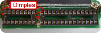
Plug the RJ45 plug into a wideband unit and measure the voltage between pins 15 and 16 of the 16-pin HIN202CP chip. It should be close to 5.0 Volts - if so then unplug the unit and insert the two chips, making very certain that the dimples on the chips match the dimples on the sockets and on the PCB. The LD02B should now power up and show something meaningful. If you have constructed the reprogramming adaptor (see below) and attach it to a source of power, and plug in the LD02B, then you should see the text "nd" to indicate power but no data. larger image.
Some basic test can be done. Press the top button to cycle through the views - the rectangular LEDs will cycle from the bottom to the top. Notice how the rectangular LEDs cycle around with each press. The view (from 0 to 3) is shown while the top button is held down. All views will show nd while there is no data from the wideband unit.
You should be able to test the function of the phototransistor. In a brightly lit room you should put your finger over the phototransistor slot. After about 10 seconds the display should have dimmed. Take your finger off and it will brighten up slowly (the slow change prevents street-light strobing). If it's not working then check the orientation of the phototransistor and make check it doesn't get brighter if you shine a torch on the phototransistor (as it should).
If your unit does not power up correctly then:
Let's assume you have found and fixed any problems, and the unit is showing nd. The utility WButil can be used to further test its functionality.
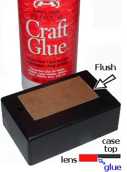
LD02 has a mechanically milled acrylic lens that is glued to the case with craft glue. Many glues (such as super glue & aircraft glues) will damage the acrylic lens. Note: the protective paper covers on the lens are left ON during gluing). 
Notice that both short edges of the lens have small projections that may need to be removed (they prevent the acrylic moving during milling) - removal can be done with a small file or 180 grit, or finer, sandpaper. Sand just enough from the lens so it fits snugly without being forced (which will also distort the case). Note that the milled hole has a small radius at each corner so chamfer the lens edges with sandpaper to fit. Insert the lens in the case so the outer side of the lens is flush with the label face. This is shown in the image (lower section) at left. The inside edges of the lens should have a lip the glue is applied to. When the fit is correct, insert the lens and apply glue to the edges of the lens from the inside ONLY. This operation is shown at right. Excess glue may spill on the paper, but it can be wiped off while the glue is still tacky. Do not remove the inside protective paper until the glue has dried. After the glue has dried and the top and bottom protective paper covers are removed, the supplied LD02 sticky label can be placed over the lens. Before exposing the label's sticky backing, do a trial run to see exactly where the label is positioned, noting that the button holes will determine the precise location. Discussion of how to use the re-programming interface is described in the |
An important feature of the LD02 is its ability to be re-programmed (reflashed) with updated firmware, and for the display to be set up for different applications. This is achieved by connecting the LD02 to a PC via the adaptor described below.
Note: A very small number of temporary adaptor PCBs were shipped in December '04 & early January '05. If you have one, then you can either have it replaced for free or build and use it - more information here.
|
|
)
)
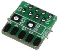
Construction is very simple. The image above right shows the bare PCB. It is labelled as TE-SER01. The three connectors are inserted from the silkscreen side. The overlay for the white Molex® connector is confusing, the top or longest lead from the connector goes to the hole labelled 12V. The female DB9 is soldered directly to the PCB noting that when oriented correctly the 4 pads on the bottom and the 5 pads on the top mate up with the DB9's solder tails. The completed adaptor is shown at left. View it as bigger popup. At right the adaptor is shown connected to a PC's RS232 cable (at left), the LD02 (at right), and the power cable from the bottom. View it as an enlarged popup. |
We continually update and amend these pages. Please see the contact link below if you find something that needs updating, is in error, or could be explained better.
)
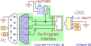
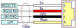
 The re-programming interface adaptor is shown in schematic format at left.
All components on the PCB are shown within the green area.
Connections to the adaptor are shown around the PCB.
The white Molex® two pin socket (top of schematic) connects to the WBo2 power cable (which we assume you are using during re-programming).
The DB9 is for connection to a PC's RS232 cable.
The LD02 itself connects to the 8 pin RJ45 connector (only the RJ45's active 4 pins are shown in the schematic).
The re-programming interface adaptor is shown in schematic format at left.
All components on the PCB are shown within the green area.
Connections to the adaptor are shown around the PCB.
The white Molex® two pin socket (top of schematic) connects to the WBo2 power cable (which we assume you are using during re-programming).
The DB9 is for connection to a PC's RS232 cable.
The LD02 itself connects to the 8 pin RJ45 connector (only the RJ45's active 4 pins are shown in the schematic).